How To Shield Plastic Housing
- LAMBDA INDIA

- Jun 15, 2019
- 4 min read
Electromagnetic fields travel through plastic electronics enclosures very easily. As a result, this type of housing is not electromagnetically compatible; in other words, electromagnetic fields generated by other equipment may interfere with the electronics, or fields emitted by the device may interfere with other electronics in the vicinity. In order to solve such problems, a shielding layer (EMI shield) will have to be applied to the plastic to make the device EMC-proof.

There are several ways to provide premium EMI/RFI shielding performance. A particular solution may be chosen depending on the attenuation desired.
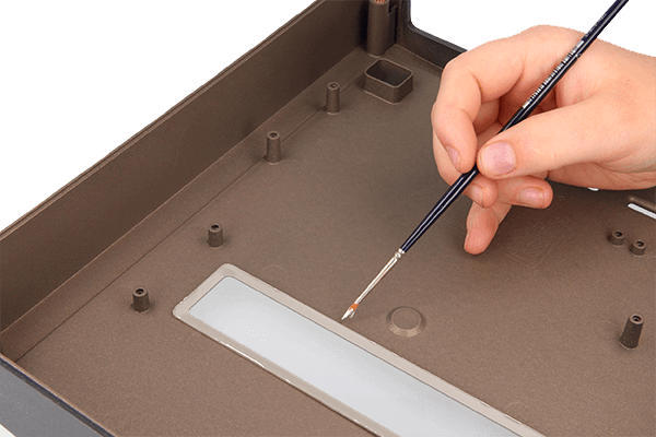
One option is painting the housing with a conductive spray, which will offer a relatively low reduction but has the advantage of being easy to apply to complex shapes. There are also films which result in higher reduction levels, but it can be difficult to apply them in housings with complex shapes.

In general:
When parts are small (up to 100 mm) and high mechanical properties are not required, a conductive plastic may be used. It is best in this case to consult with your moulder and us in order to find the best possible solution.
With a galvanic or chemical treatment (for small parts and large quantities), generally speaking, a selective coating is not possible. Both the inside and the outside are treated.
Shielding Vents Design:
The key to properly shielding enclosures around openings is controlling the size and depth of the opening in relation to the operating frequency of the device. The relationship is the basis for an EMI shielding technique known as the wave-guide effect (See Calculating cutoff frequency as described below) which can either support or attenuate the EMI.
When designing vents and apertures, use the following guidelines:
• To avoid antenna effects and attenuate EMI, make sure the distance across an opening is less than half of the signal wavelength
(typical values fall in the range from 1⁄4 to 1⁄5 the expected wavelength).
• Use a greater number of small openings rather than one large opening. It is better to have several rows of smaller vents than one row of large vents.
• Frequency requirements for both emitted and incoming EMI must be considered for enclosure designs. Leakage potential increases as frequencies increase (or wavelength decreases), which reduces the allowable discontinuity length.
• Leakage also depends on EMI wave impedance and direction. It is important to define whether a wave is predominantly electric, magnetic, or planar, as well as the distance between the radiating source and the opening.
Grounding:
With faster processing speeds, today’s electronics produce electronic fields that build and fade rapidly, which can lead to interference. Adequate grounding is necessary to control the electromagnetic charges. More compact designs, as well as the increased use of electronic devices, also make field interactions a concern.
Engineers commonly rely on fasteners to create a common ground between mating parts. To maximize contact between two parts, use bosses to enclose screw threads. This helps increase clamping forces as well as protecting fasteners from oxidation.
Coating requirements for grounds are similar to those for snap fits and contact fingers. Maintaining surface conductivity is the key to effective shielding. If the coating’s conductivity decreases due to oxidation or corrosion, resistance increases across mating surfaces which will lead to EMI.
Ground designs range from relatively simple to fairly complex depending on the enclosure configuration. However, for more complex designs, electroless plating or automated paint systems are needed to provide uniform coating coverage. By using properly applied conductive coatings, extensive ground-plane strapping, clips, gaskets, and bonding straps can be reduced.
Gasketing:
Use gaskets between mating parts, followed by the application of conductive coating to handle EMI. Uniform coverage of the conductive coating not only helps ground parts, but also eliminates the need for gaskets. The selection of a given coating process should take into consideration its ability to fill the narrow gaps left between mating parts.
CALCULATING CUTOFF FREQUENCY
The relationship between the size and depth of a gap, seam, or hole, and the device’s operating frequency affects a components ability to shield EMI. The relationship between these parameters is known as the wave-guide effect. Wave guides such as vents and holes have a cutoff frequency, vc, below which it becomes an attenuator, according to: fc (Hz) = c/λc where λc = 2 times the maximum dimension (for slots) = 1.7 times the diameter (for holes) and c = speed of light = 3.0 × 10⁸ m/sec.
When the signal frequency is below the cutoff frequency of the wave guide — in other words the signal wavelength is longer than the wave-guide cutoff
wavelength — the theoretical attenuation of the wave guide is: SE (dB) = 27.3 d/w (for slots) = 32.0 d/D (for holes) where d = depth of the opening w = width of the opening D = diameter of the hole
For example, a 0.25-in.-diameter hole has a cutoff frequency of 2.8 GHz and a corresponding cutoff wavelength of 0.43 in. A 1-in. slot has a v = 600 MHz and a λ = 2 in.
To preventing EMI leaking from vents and apertures, use the following guidelines: λ< 2d — radiation passes freely λ = 2d — cutoff frequency, no EMI shielding λ> 2d — effective shielding Multiple vent spacing should be at least ½λ (λ/2 > d)
Recommendations from LAMBDA INDIA:
First choice for a shielded enclosure should be a metallic enclosure, such as an aluminum box. In order to get good shielding at high frequencies, the conductivity between the lid and the box must be close to Zero, and the joint between the lid and box should have a baffle to prevent leakage.
If a metallic box is not feasible, the use of a conductive plastic enclosure will provide shielding. Hammond uses two methods of shielding, Conductive Paint, and Conductive Plastic.
Conductive Plastic is the best solution for some styles of plastic enclosures. The plastic is compounded with stainless steel fibers, forming a three dimensional conductive matrix inside the base material. This method provides a consistent enclosure, with no secondary coating quality issues.
The shielded enclosures have almost identical physical properties to the unshielded equivalent, Esthetics, Strength, etc. The material is UL94 – V0.
In order to EMC-shield a plastic housing, the following solutions are available:
- Electrically conductive nickel coating.
- Electrically conductive metallization.
- Mu-copper housings and enclosures for EMI shielding of PCBs inside a plastic housing.
- High-precision conductive EMI foil shaping.
If you would like to receive advice (free of charge), please send your drawing by e-mail to LAMBDA INDIA . We will answer within a few hours.
Author -
LAMBDA INDIA


Comments